Application Note (25)
-
M68HC08 to HCS08 Transition[AN2717]
-
MC9S08GB/GT Low Power Modes[AN2493]
-
Serial Monitor for MC9S08GB/GT[AN2140]
Application Note Software (12)
-
AN3315SW[AN3315SW]
-
Software for AN2616[AN2616SW]
-
Software Files for AN2494[AN2494SW]
-
Software to Accompany AN2949[AN2949SW1]
Brochure (1)
-
GT16A and ZigBee Brochure[8BITZIGBEEFS.PDF]
Data Sheet (4)
-
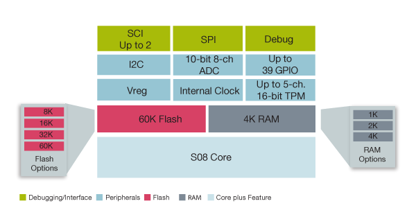
MC9S08GB60A, MC9S08GB32A, MC9S08GT60A, MC9S08GT32A - Data Sheet[MC9S08GB60A]Featured
-
MC9S08GT16A, MC9S08GT8A - Data Sheet[MC9S08GT16A]Featured
-
MC9S08GB32, MC9S08GT60, MC9S08GT32, MC9S08GT16 - Data Sheet[MC9S08GB60]Featured
Errata (8)
-
Mask Set Errata: 2M70C - Errata[MSE9S08GT16A_2M70C]
-
Mask Set Errata: 4L11Y - Errata[MSE9S08GB60A_4L11Y]
-
Mask Set Errata: 3L31R - Errata[MSE9S08GB60_3L31R]
-
Mask Set Errata: 4L31R - Errata[MSE9S08GB60_4L31R]
-
Mask Set Errata: 3L11Y - Errata[MSE9S08GB60A_3L11Y]
-
Mask Set Errata: 2L31R - Errata[MSE9S08GB60_2L31R]
-
Mask Set Errata: 1L31R - Errata[MSE9S08GB60_1L31R]
Fact Sheet (3)
-
8-Bit Consumer and Industrial Product List[8BITCIPRODMPFS.PDF]
-
9S08GT60/GT32/GT16[9S08GT603216FS]Featured
-
MC9S08GT16A/8A - Fact Sheet[MC9S08GT16AFS]Featured
Product Change Notice (2)
Reference Manual (2)
Reliability and Quality Information (3)
-
VDE IEC 60730 Class B test report for the MC9S08 MCU[VDE_S08_CLASSB_TEST_REPORT]
-
Tuev IEC 60730 CPU test certificate for MC9S08 controller[TUEVCPUCLASSCCERT]
-
Tuev IEC 60730 SRAM test certificate for MC9S08 controller[TUEVCERTIFICATIONWALKPATRAM]