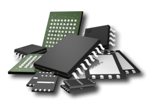
8-bit Flexis QE MCUs
Design Files
Receive the full breakdown. See the product footprint and more in the eCad file.
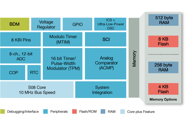
NXP® understands the challenge of performance within an energy budget and offers a wide portfolio of S08 devices that help you reach target performance levels while minimizing low-power in your design. The S08QB family demonstrates extreme energy-efficiency for ultra-long operating life in battery-powered applications.
8-bit Flexis QE MCUs
|
|
|
|
|
|
|
|---|---|---|---|---|---|
|
|
|
|
|
|
|
|
|
|
|
|
|
|
|
|
|
|
|
|
|
|
|
|
|
|
|
|
|
|
|
|
|
|
|
|
|
|
|
|
|
|
|
|
|
|
|
|
|
|
|
|
|
|
|
|
|
|
|
|
|
|
|
|
|
|
|
|
|
|
Quick reference to our documentation types.
1-10 of 40 documents
Compact List
Receive the full breakdown. See the product footprint and more in the eCad file.
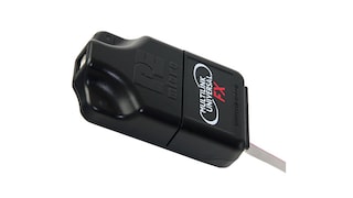
4 hardware offerings
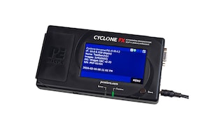
Additional hardware available. View our featured partner solutions.
Quick reference to our software types.
1-5 of 10 software files
Additional software available. View our featured partner solutions.
Note: For better experience, software downloads are recommended on desktop.
To get further assistance directly from NXP, please see our Engineering Services.
2 engineering services

To find additional partner offerings that support this product, visit our Partner Marketplace.