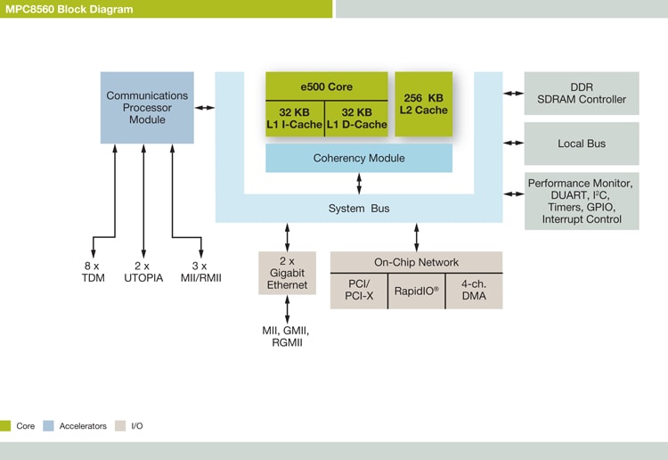
PowerQUICC® III Processor with TDM, DDR, PCI, PCIx Express®, RapidIO, 1 GB Ethernet, Security, CPM with UTOPIA

  • This page contains information on a product that is not recommended for new designs.

Block Diagram

Freescale PowerQUICC MPC8560 Communications Processor Block Diagram

PowerQUICC<sup>&#174;</sup> MPC8560 Communications Processor Block Diagram

Features

  • 32-bit, dual-issue, superscalar, seven-stage pipeline
  • 1850 MIPS at 800 MHz (est. Dhrystone 2.1)
  • 32 KB L1 data and 32 KB L1 instruction cache with line locking support
  • 256 KB on-chip L2 cache with direct mapped capability
  • Enhanced hardware and software debug support
  • Memory management unit (MMU)
  • SIMD extension with single precision floating point
  • High-performance RISC CPM available at up to 333 MHz
    • CPM software compatibility with previous families
    • Greater than 1 Gbps aggregate CPM bandwidth
    • 32 KB of dual-port RAM
    • 128 KB of ROM + 32 KB of RAM for protocol microcode storage
    • Two UTOPIA Level II leader/follower ports with multi-PHY support (one can be 16-bit)
    • Three MII interfaces
    • Eight TDM interfaces (T1/E1), two TDM ports that can be interfaced with T3/E3
    • Four SCCs supporting HDLC and SDLC, HDLC bus, UART, Transparent, BISYNC
    • Three FCCs supporting:
      • Up to 155 Mbps ATM SAR-AAL0, AAL1, AAL2, AAL3/4, AAL5
      • 10/100 Mbps Ethernet (up to three) IEEE® 802.3X
      • 45 Mbps HDLC/transparent (up to three)
    • Two MCCs each supporting 128 full-duplex, 64 kbps, HDLC lines for a total of 256 channels
    • ATM transmission convergence layer capabilities (8 channels)
    • Integrated inverse multiplexing for ATM (IMA) functionality
  • Two triple-speed Ethernet controllers (TSECs) supporting 10/100/1000 Mbps Ethernet (IEEE 802.3, 802.3u, 802.3x, 802.3z, and 802.3ac compliant) with two GMII/TBI/RGMII interfaces
  • 166 MHz, 64-bit, 2.5V I/O, DDR SDRAM memory controller with full ECC support
  • 500 MHz, 8-bit, LVDS I/O, RapidIO controller
  • 133 MHz, 64-bit, 3.3V I/O, PCI-X 1.0a/PCI 2.2 bus controller
  • 166 MHz, 32-bit, 3.3V I/O, local bus with memory controller
  • Integrated four-channel DMA controller
  • Interrupt controller
  • IEEE 1149.1 JTAG test access port
  • 1.2V core power supply with 3.3V and 2.5V I/O
  • 783-pin FC-BGA package
  • This product is included in NXP®.s product longevity program, with assured supply for a minimum of 10 years after launch
  • Buy/Parametrics


    Documentation

    Quick reference to our documentation types.

    1-10 of 68 documents

    Compact List

    Application Note (42)
    Application Note Software (8)
    Data Sheet (1)
    Fact Sheet (1)
    Package Information (1)
    Product Brief (2)
    Reference Manual (7)
    Technical Notes (1)
    User Guide (1)
    White Paper (4)

    Design Files

    Quick reference to our design files types.

    2 design files

    Hardware

    Quick reference to our board types.

    2 hardware offerings

    Software

    Quick reference to our software types.

    5 software files

    Note: For better experience, software downloads are recommended on desktop.

    Support

    What do you need help with?