MPC8548 device is "Not recommended for new designs", please use the replacement families Power Architecture (T1023, T1040 ,T1042),
Arm Architecture (LS1023A).
Our next-generation PowerQUICC® III processors are based on the scalable e500 system-on-chip (SoC) platform and Power Architecture® processor core. These PowerQUICC III processors, the MPC8548E, MPC8547E, MPC8545E and MP8543E, are designed to deliver gigahertz-plus communications processing performance and advanced features with integration and high-speed connectivity required by enterprise networking, telecom transmission and switching, 3G wireless infrastructure, storage and high-end imaging markets.. The processors are designed to offer clock speeds scaling up to 1.5 GHz. They combine the powerful processor core, enhanced peripherals and high-speed interconnect technology to balance processor performance with I/O system throughput.
The next-generation PowerQUICC III processors are based on our 90 nanometer (nm) silicon-on-insulator (SOI) copper interconnect process technology, which enables processors to deliver higher performance with lower power dissipation. At 1.5 GHz, these processors deliver a significant performance increase over 130 nm PowerQUICC III devices, adding another level of great performance and uncompromising integration to the PowerQUICC family.
The MPC8548E, MPC8547E, MPC8545E and MP8543/E processors offer a wide range of high-speed connectivity options, including Gigabit Ethernet (GbE), Serial RapidIO® technology and PCI Express®. Support for these high-speed interfaces enables scalable connectivity to network processors and/or ASICs in the data plane while the PowerQUICC III handles complex, computationally demanding control plane processing tasks. These processors also feature next-generation double data rate (DDR) memory controller, enhanced, GbE support, double precision floating point and integrated security engines that support the Kasumi alogrithm needed for 3G wireless security. In addition, support is provided for exclusive or XOR acceleration needed for parity in storage applications.
The 8543E, 8545E, 8547E, and 8548E: Application-Specific and Market-Driven
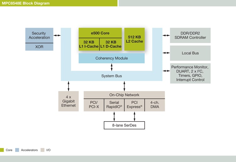
MPC8548E networking/telecom processor—Key features include 512 KB L2 cache, integrated security engine, 64-bit DDR/DDR2 scaling to 533 MHz data rate, dual 32-bit PCI or 64-bit PCI-X, 4-bit Serial RapidIO fabric technology and 4-bit PCI-Express (or single 8-bit PCI Express 1.0a), local bus IO interfaces, and four GbE interfaces. The combination of these features makes this device an optimal communications processing solution for Ethernet-only or RapidIO interworking applications, such as enterprise networking, telecom transmission and switching and 3G wireless base stations. The security engine includes Kasumi algorithm acceleration, making the MPC8548E an ideal choice for enhancing security protocol processing in 2.5G and 3G wireless network infrastructure.
MPC8547E storage processor—Key features include 512 KB L2 cache, integrated security acceleration with XOR capability, support for battery-backed 64-bit DDR/DDR2 scaling to 533 MHz data rate, 64-bit PCI-X, 8-bit PCI Express and four GbE interfaces. The device's XOR acceleration enhances system performance by offloading the compute-intensive parity checks in small-medium business and enterprise redundant array of inexpensive disks (RAID) storage applications.
MPC8545E imaging processor—Key features include 512 KB L2 cache, 64-bit DDR/DDR2 scaling up to 533 MHz data rate, integrated security, dual 32-bit PCI/single 64-bit PCI, 4-bit PCI Express and two GbE interfaces. The MPC8545E also offers double precision floating point, a capability that makes this device a high-performance processing solution for a wide range of imaging applications.
MPC8543E general-purpose control processor—Key features include 256 KB L2 cache, integrated security, 64-bit DDR/DDR2 scaling up to 400 MHz data rate, 32-bit PCI, 4-bit Serial RapidIO or 4-bit PCI Express, and two GbE interfaces. With clock frequencies scaling from 800 MHz to 1 GHz, this cost-effective device is ideally suited for a wide range of general-purpose embedded control applications, such as robotics, discrete manufacturing and process manufacturing control.
Contact your local NXP® Sales Office or NXP Authorized Distributor.