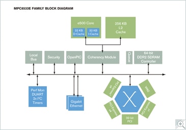
MPC8533E PowerQUICC® III Processor

  • MPC8533 device is "Not recommended for new designs", please use the\n replacement families Power Architecture (T1013,\n T1023),\n Arm Architecture (LS1012A, LS1023A).

Block Diagram

MPC8533E Block Diagram

Features

  • Embedded e500 core, initial offerings up to 667 MHz, targeting up to 1.0 GHz
    • Dual dispatch superscalar, 7-stage pipeline design with out-of-order issue and execution
    • 2,240 MIPS at 1.0 GHz (estimated Dhrystone 2.1)
    • 36-bit physical addressing
  • Enhanced hardware and software debug support
  • Double-precision embedded scalar and vector floating-point APUs
  • Memory management unit (MMU)
  • Double-precision embedded scalar and vector floating-point APUs
  • Integrated L1/L2 cache
    • L1 cache—32 KB data and 32 KB instruction cache with line-locking support
    • L2 cache—256 KB (8-way set associative); 256/128/64/32 KB can be used as SRAM
    • L1 and L2 hardware coherency
    • L2 cache and I/O transactions can be stashed into L2 cache regions
  • Integrated DDR memory controller with full ECC support, offering:
    • 200 MHz clock rate (400 MHz data rate), 64-bit, 2.5V/2.6V I/O, DDR SDRAM
    • 267 MHz clock rate (up to 533 MHz data rate), 64-bit, 1.8V I/O, DDR2 SDRAM
  • Integrated security engine supporting DES, 3DES, MD-5, SHA-1/2, AES, RSA, RNG, Kasumi F8/F9 and ARC-4 encryption algorithms
  • Two on-chip Three Speed Ethernet controllers (ETSECs) supporting 10 Mbps, 100 Mbps and 1 Gbps Ethernet/IEEE® 802.3 networks with MII, RMII, RGMII, and RTBI physical interfaces:
    • TCP/UDP/IP checksum acceleration
    • Advanced QoS features
  • General-purpose input/output (GPIO)
  • PCI Express high-speed interconnect interfaces, supporting combinations of dual x4 and single x1 PCI Express
  • On-chip network (OCeaN) switch fabric
  • PCI interface support
    • 32-bit PCI 2.2 bus controller (up to 66MHz, 3.3V I/O)
  • Local bus
    •  166 MHz, 32-bit, 3.3V I/O, local bus with memory controller
  • Integrated four-channel DMA controller
    •  Multiplexed 32-bit address and data operating up to 133 MHz
    •  32-, 16- and 8-bit port sizes controlled by on-chip memory controller
  • Dual I²C and DUART support
  • Dual I²C interfaces (controller or target mode)
  • Programmable interrupt controller (PIC)
  • IEEE 1149.1 JTAG test access port
  • 1.0V core voltage with 3.3V and 2.5V I/O
  • 783-pin FC-BGA package
  • Buy/Parametrics


    Documentation

    Quick reference to our documentation types.

    1-10 of 49 documents

    Compact List

    Application Note (28)
    Application Note Software (4)
    Data Sheet (1)
    Fact Sheet (2)
    Package Information (2)
    Product Brief (1)
    Reference Manual (5)
    Supporting Information (2)
    White Paper (4)

    Design Files

    Quick reference to our design files types.

    1 design file

    Hardware

    Quick reference to our board types.

    2 hardware offerings

    Software

    Quick reference to our software types.

    3 software files

    Note: For better experience, software downloads are recommended on desktop.

    Engineering Services

    1-5 of 6 engineering services

    Show All

    To find additional partner offerings that support this product, visit our Partner Marketplace.

    Training

    6 trainings

    Show All

    Support

    What do you need help with?