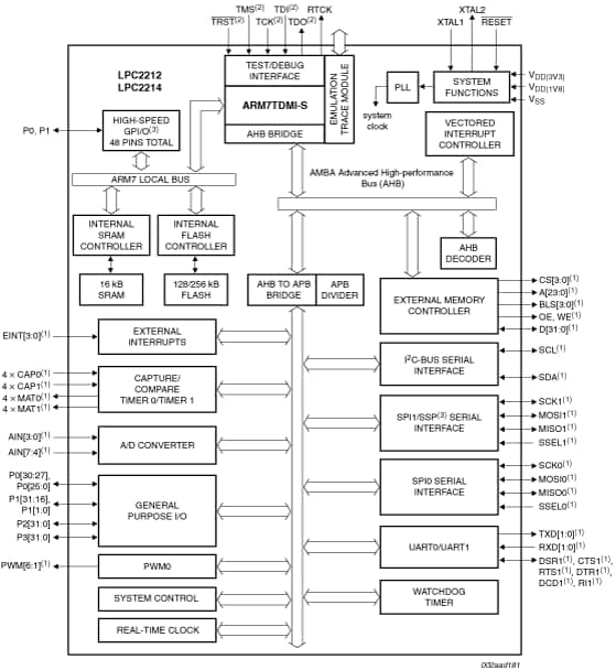
Single-chip 16/32-bit Arm® microcontrollers; 128/256 kB ISP/IAP flash with 10-bit ADC and external memory interface

  • This page contains information on a product that is not recommended for new designs.

See product image

Product Details

Block Diagram

Block diagram: LPC2212FBD144, LPC2214FBD144

Features

2.1 Key features brought by LPC2212/2214/01 devices
  • Fast GPIO ports enable port pin toggling up to 3.5 times faster than the original device. They also allow for a port pin to be read at any time regardless of its function.
  • Dedicated result registers for ADC(s) reduce interrupt overhead. The ADC pads are 5 V tolerant when configured for digital I/O function(s).
  • UART0/1 include fractional baud rate generator, auto-bauding capabilities and handshake flow-control fully implemented in hardware.
  • Buffered SSP serial controller supporting SPI, 4-wire SSI, and Microwire formats.
  • SPI programmable data length and leader mode enhancement.
  • Diversified Code Read Protection (CRP) enables different security levels to be implemented. This feature is available in LPC2212/2214/00 devices as well.
  • General purpose timers can operate as external event counters.

2.2 Key features common for all devices

  • 16/32-bit Arm7TDMI-S microcontroller in a LQFP144 package.
  • 16 kB on-chip static RAM and 128/256 kB on-chip flash program memory. 128-bit wide interface/accelerator enables high speed 60 MHz operation.
  • In-System Programming (ISP) and In-Application Programming (IAP) via on-chip bootloader software. Flash programming takes 1 ms per 512 B line. Single sector or full chip erase takes 400 ms.
  • EmbeddedICE-RT and Embedded Trace interfaces offer real-time debugging with the on-chip RealMonitor software as well as high speed real-time tracing of instruction execution.
  • Eight-channel 10-bit ADC with conversion time as low as 2.44 µs.
  • Two 32-bit timers (with four capture and four compare channels), PWM unit (six outputs), Real-Time Clock and Watchdog.
  • Multiple serial interfaces including two UARTs (16C550), Fast I²C-bus (400 kbit/s) and two SPIs.
  • Vectored Interrupt Controller with configurable priorities and vector addresses.
  • Configurable external memory interface with up to four banks, each up to 16 MB and 8/16/32-bit data width.
  • Up to 112 general purpose I/O pins (5 V tolerant). Up to nine edge or level sensitive external interrupt pins available.
  • 60 MHz maximum CPU clock available from programmable on-chip Phase-Locked Loop with settling time of 100 µs.
  • On-chip crystal oscillator with an operating range of 1 MHz to 30 MHz.
  • Two low power modes, Idle and Power-down.
  • Processor wake-up from Power-down mode via external interrupt.
  • Individual enable/disable of peripheral functions for power optimization.
  • Dual power supply:
    • CPU operating voltage range of 1.65 V to 1.95 V (1.8 V ± 0.15 V).
    • I/O power supply range of 3.0 V to 3.6 V (3.3 V ± 10 %) with 5 V tolerant I/O pads.

Buy/Parametrics


Documentation

Quick reference to our documentation types.

1-10 of 26 documents

Compact List

Application Note (16)
Brochure (1)
Data Sheet (1)
Errata (2)
Package Information (1)
Supporting Information (4)
User Guide (1)

Design Files

Quick reference to our design files types.

1 design file

Software

Quick reference to our software types.

1 software file

Note: For better experience, software downloads are recommended on desktop.

Support

What do you need help with?