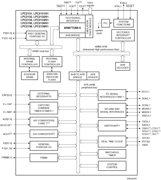
Single-chip 16/32-bit microcontrollers; 32/64/128/256/512 kB ISP/IAP flash with 10-bit ADC and DAC

  • This page contains information on a product that is not recommended for new designs.

See product image

Product Details

Block Diagram

Block diagram: LPC2131FBD64, LPC2132FBD64, LPC2132FHN64, LPC2134FBD64, LPC2136FBD64, LPC2138FBD64, LPC2138FHN64

Features

2.1 Enhancements brought by LPC213x/01 devices
  • Fast GPIO ports enable port pin toggling up to 3.5 times faster than the original LPC213x. They also allow for a port pin to be read at any time regardless of its function.
  • Dedicated result registers for ADC(s) reduce interrupt overhead.
  • UART0/1 include fractional baud rate generator, auto-bauding capabilities and handshake flow-control fully implemented in hardware.
  • Additional BOD control enables further reduction of power consumption.

2.2 Key features common for LPC213x and LPC213x/01

  • 16/32-bit Arm7TDMI-S microcontroller in a tiny LQFP64 or HVQFN64 package.
  • 8/16/32 kB of on-chip static RAM and 32/64/128/256/512 kB of on-chip flash program memory. 128-bit wide interface/accelerator enables high-speed 60 MHz operation.
  • In-System Programming/In-Application Programming (ISP/IAP) via on-chip bootloader software. Single flash sector or full chip erase in 400 ms and programming of 256 B in 1 ms.
  • EmbeddedICE RT and Embedded Trace interfaces offer real-time debugging with the on-chip RealMonitor software and high-speed tracing of instruction execution.
  • One (LPC2131/32) or two (LPC2134/36/38) 8-channel 10-bit ADCs provide a total of up to 16 analog inputs, with conversion times as low as 2.44 µs per channel.
  • Single 10-bit DAC provides variable analog output (LPC2132/34/36/38).
  • Two 32-bit timers/external event counters (with four capture and four compare channels each), PWM unit (six outputs) and watchdog.
  • Low power Real-time clock with independent power and dedicated 32 kHz clock input.
  • Multiple serial interfaces including two UARTs (16C550), two Fast I²C-bus (400 kbit/s), SPI and SSP with buffering and variable data length capabilities.
  • Vectored interrupt controller with configurable priorities and vector addresses.
  • Up to forty-seven 5 V tolerant general purpose I/O pins in tiny LQFP64 or HVQFN package.
  • Up to nine edge or level sensitive external interrupt pins available.
  • 60 MHz maximum CPU clock available from programmable on-chip PLL with settling time of 100 µs.
  • On-chip integrated oscillator operates with external crystal in range of 1 MHz to 30 MHz and with external oscillator up to 50 MHz.
  • Power saving modes include Idle and Power-down.
  • Individual enable/disable of peripheral functions as well as peripheral clock scaling down for additional power optimization.
  • Processor wake-up from Power-down mode via external interrupt or BOD.
  • Single power supply chip with POR and BOD circuits:
    • CPU operating voltage range of 3.0 V to 3.6 V (3.3 V ± 10 %) with 5 V tolerant I/O pads.

Buy/Parametrics


Documentation

Quick reference to our documentation types.

1-10 of 29 documents

Compact List

Application Note (20)
Data Sheet (1)
Errata (2)
Package Information (1)
Packing Information (1)
Supporting Information (3)
User Guide (1)

Design Files

Quick reference to our design files types.

3 design files

Software

Quick reference to our software types.

2 software files

Note: For better experience, software downloads are recommended on desktop.

Support

What do you need help with?