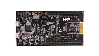
Fully Certified Module Supporting Bluetooth and NFC
Design Files
Receive the full breakdown. See the product footprint and more in the eCad file.
Note: QN9090/30 is preferred for any new Bluetooth LE design.
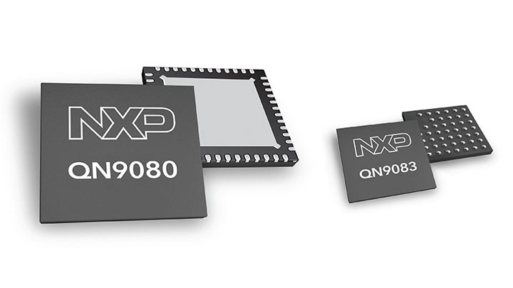
QN908x is an ultra-low-power, high-performance and highly integrated Bluetooth Low Energy solution for Bluetooth® Smart applications such as sports and fitness, human interface devices, and app-enabled smart accessories. It is specially designed for wearable electronics with a small capacity battery.
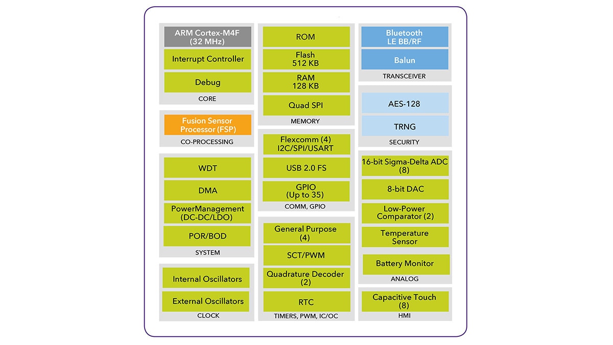
QN908x integrates a Bluetooth Low-Energy radio, controller, protocol stack and profile software on a single chip, providing a flexible and easy to use Bluetooth Low Energy SoC solution. It also includes a high-performance MCU (32-bit Arm® Cortex®-M4F), on-chip memory, and peripherals for users to develop a truly single-chip wireless solution.
Additional system features include fully integrated DC-DC and LDO, low power sleep timer, battery monitor, 16-bit high-resolution general purpose ADC, and GPIOs, to further reduce overall system size and cost. QN908x operates with a power supply range of 1.8 V to 3.6 V and has very low power consumption in all modes. It enables long lifetime in battery-operated systems while maintaining excellent RF performance.
Fully Certified Module Supporting Bluetooth and NFC
|
|
|
|
|
|
|
|---|---|---|---|---|---|
|
|
|
|
|
|
|
|
|
|
|
|
|
|
|
|
|
|
|
|
|
|
|
|
|
|
|
|
|
|
|
|
|
|
|
|
|
|
|
|
|
|
|
|
|
|
|
|
|
|
|
|
|
|
|
|
|
|
|
|
|
|
|
|
|
|
|
|
|
|
Quick reference to our documentation types.
1-10 of 28 documents
Compact List
Receive the full breakdown. See the product footprint and more in the eCad file.
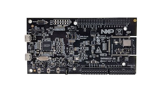
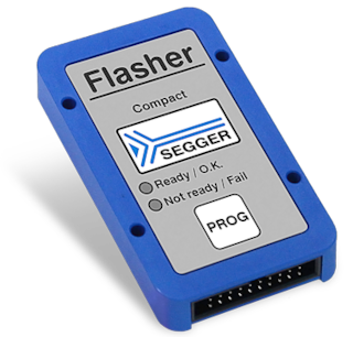
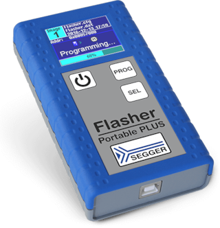
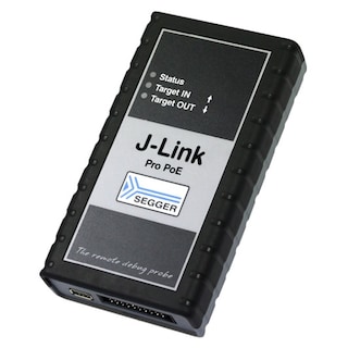
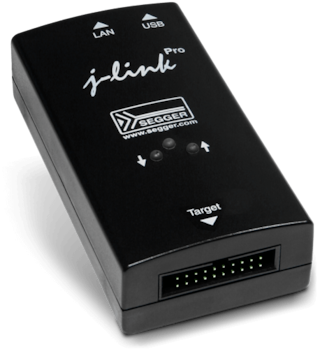
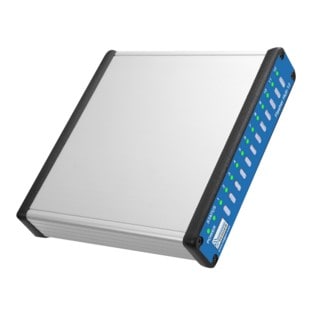
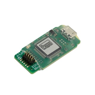
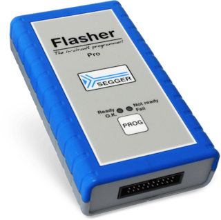
1-5 of 6 hardware offerings
Additional hardware available. View our featured partner solutions.
Quick reference to our software types.
1-5 of 10 software files
Additional software available. View our featured partner solutions.
Note: For better experience, software downloads are recommended on desktop.
To get further assistance directly from NXP, please see our Engineering Services.
3 engineering services


To find additional partner offerings that support this product, visit our Partner Marketplace.