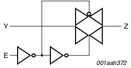
Low-Ohmic Single-Pole Single-Throw Analog Switch

  • This page contains information on a product that is no longer manufactured (discontinued). Specifications and information herein are available for historical reference only.

Block Diagram

Choose a diagram:

NX3L1G66/Q100 Block Diagram

NX3L1G66, Q100 Block Diagram

NX3L2G66; logic diagram

NX3L2G66; logic diagram

Features

Key Features

  • Wide supply voltage range from 1.4 V to 4.3 V
  • Very low ON resistance (peak):
    • 1.6 Ω (typical) at VCC = 1.4 V
    • 1.0 Ω (typical) at VCC = 1.65 V
    • 0.55 Ω (typical) at VCC = 2.3 V
    • 0.50 Ω (typical) at VCC = 2.7 V
    • 0.50 Ω (typical) at VCC = 4.3 V
  • High noise immunity
  • ESD protection:
    • HBM JESD22-A114E Class 3A exceeds 7500 V
    • MM JESD22-A115-A exceeds 200 V
    • CDM AEC-Q100-011 revision B exceeds 1000 V
  • CMOS low-power consumption
  • Latch-up performance exceeds 100 mA per JESD 78 Class II Level A
  • Direct interface with TTL levels at 3.0 V
  • Control input accepts voltages above supply voltage
  • High current handling capability (350 mA continuous current under 3.3 V supply)
  • Specified from -40 Cel to +85 Cel and from -40 Cel to +125 Cel

Buy/Parametrics


Documentation

Quick reference to our documentation types.

10 documents

Compact List

Application Note (1)
Data Sheet (1)
Package Information (2)
Packing Information (3)
Supporting Information (3)

Design Files

Quick reference to our design files types.

1 design file

Support

What do you need help with?